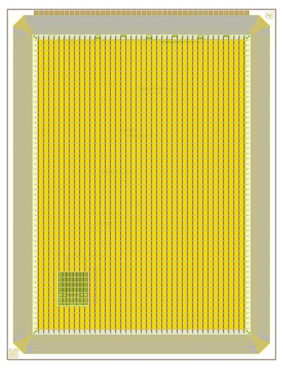
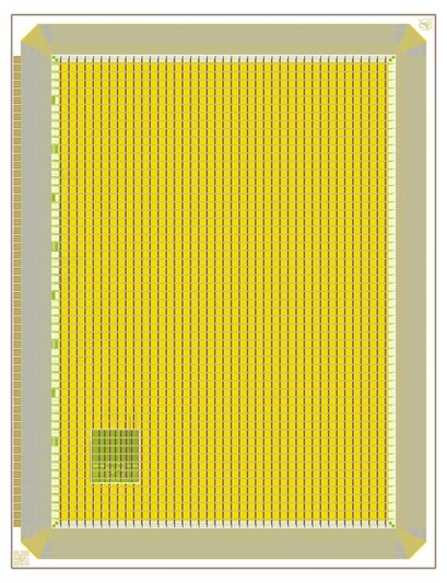
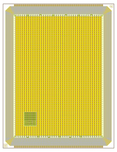
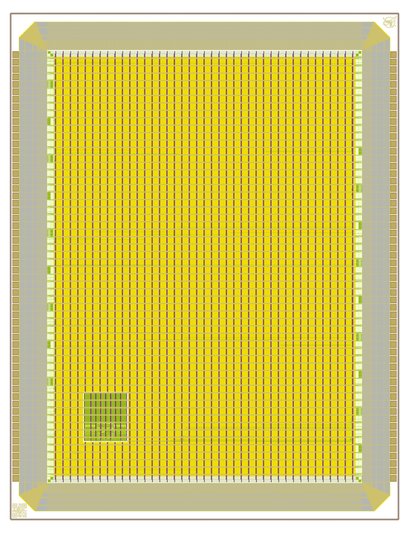
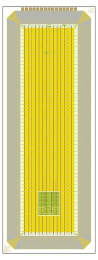
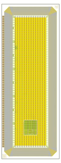
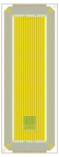
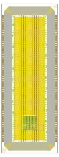
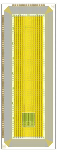
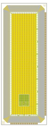
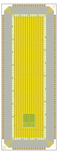
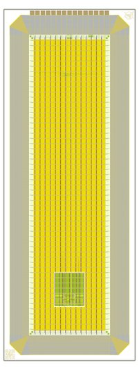
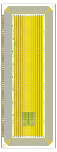
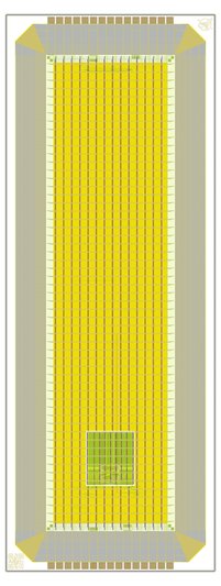
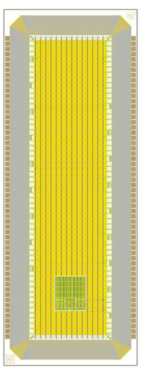
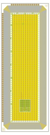
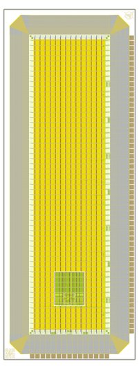
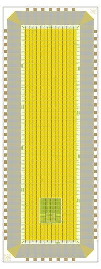
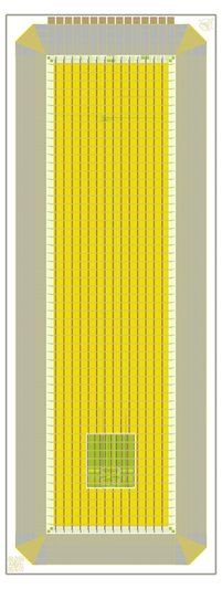
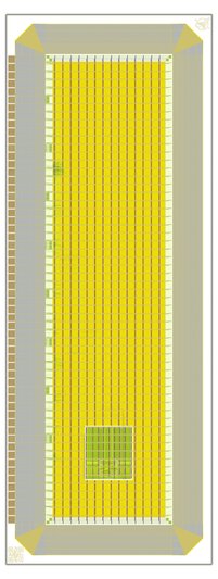
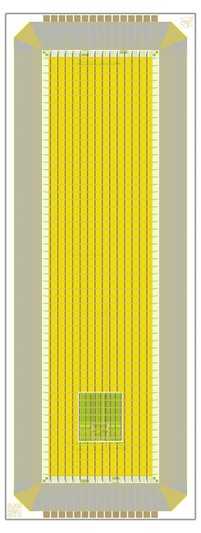
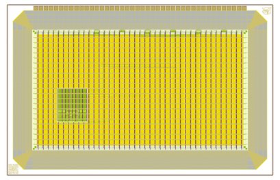
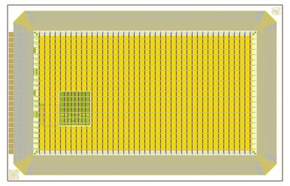
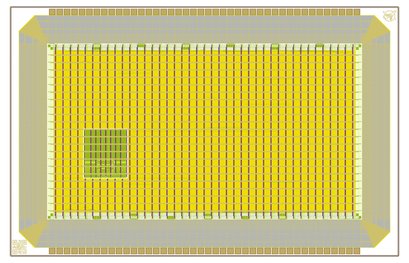
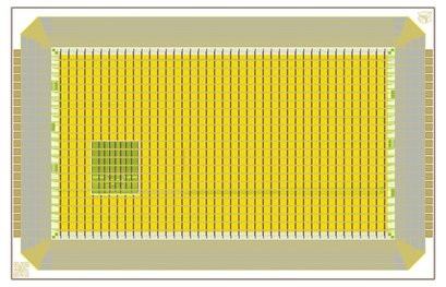
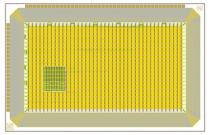
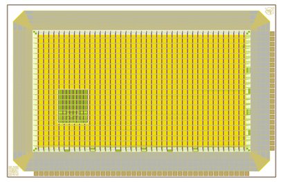
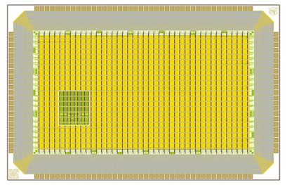
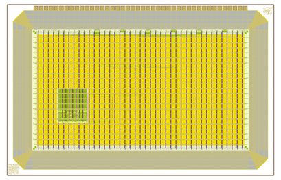
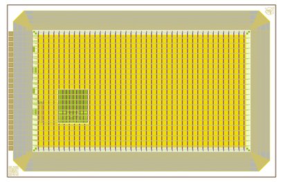
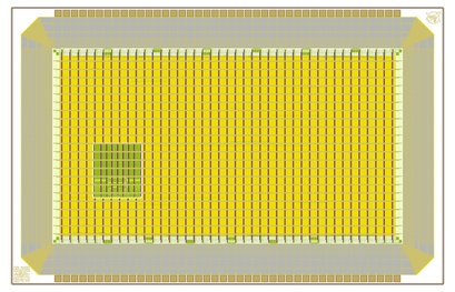
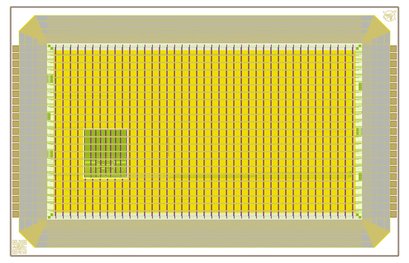
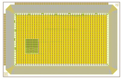
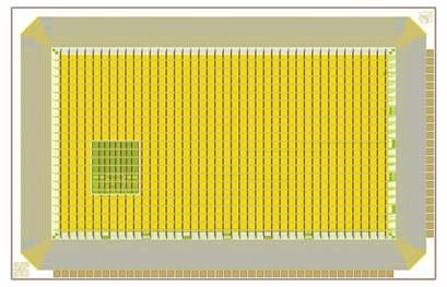
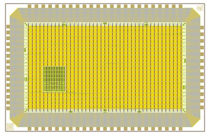
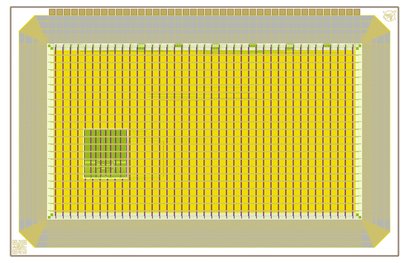
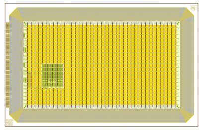
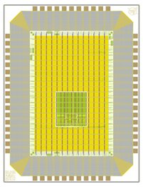
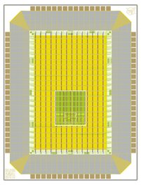
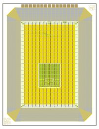
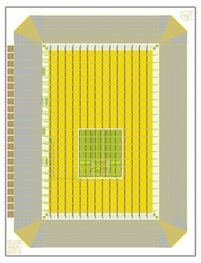
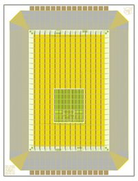
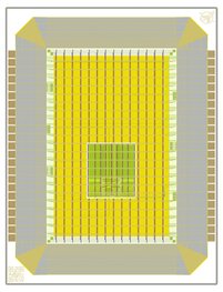
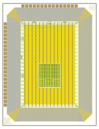
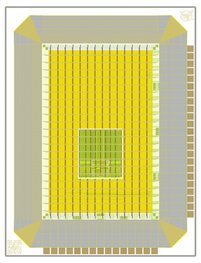
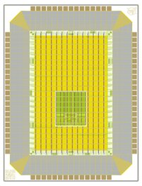
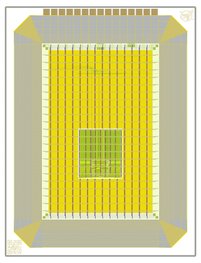
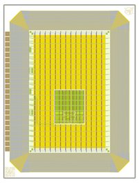
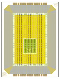
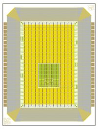
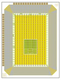
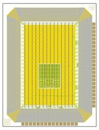
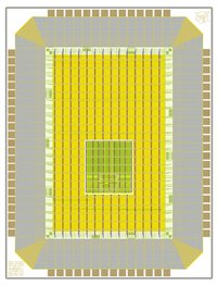
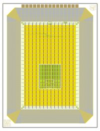
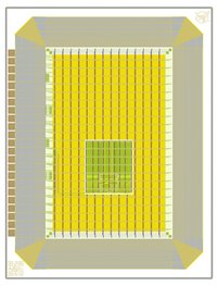
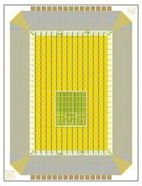
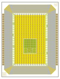
GF180MCU Slot Sizes

wafer.space Project Template | GitHub | Generated: 20 May 2026 12:07 UTC

Standard Slot Configurations

Available Slots

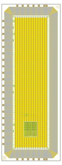
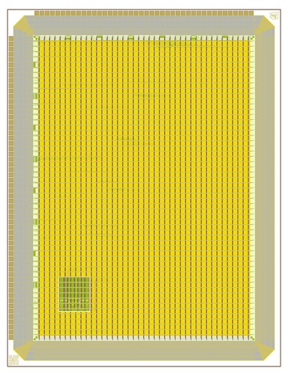
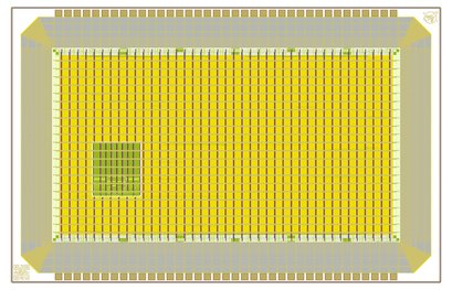
1×1 (Full)
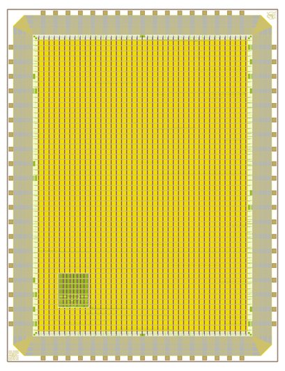
1×1 (Full)
Die Size
3.93mm × 5.12mm (20.14mm²)
Usable Silicon
3.88mm × 5.07mm (19.67mm²)
Core Area
3.05mm × 4.24mm (12.92mm²)
IO Overhead
36%
Total IOs
56 (bidir: 40, in: 14, analog: 2)
Power Pads
18 (8 DVDD + 10 DVSS)
Total Pads
74 (56 IO + 18 power)

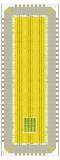
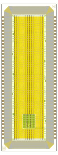
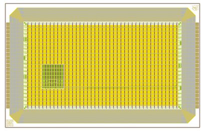
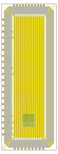
0.5×1 (Half Width)
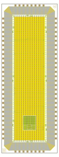
0.5×1 (Half Width)
Die Size
1.94mm × 5.12mm (9.92mm²)
Usable Silicon
1.88mm × 5.07mm (9.55mm²)
Core Area
1.05mm × 4.24mm (4.46mm²)
IO Overhead
55%
Total IOs
56 (bidir: 44, in: 6, analog: 6)
Power Pads
16 (8 DVDD + 8 DVSS)
Total Pads
72 (56 IO + 16 power)

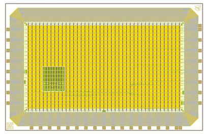
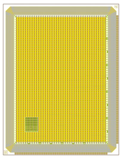
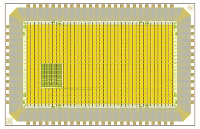
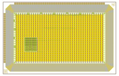
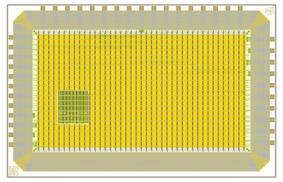
1×0.5 (Half Height)
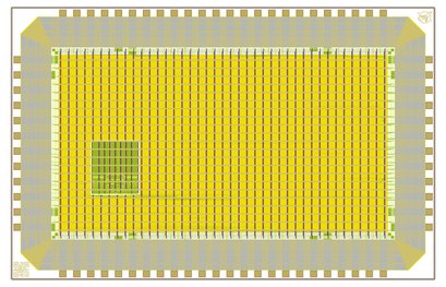
1×0.5 (Half Height)
Die Size
3.93mm × 2.53mm (9.95mm²)
Usable Silicon
3.88mm × 2.48mm (9.62mm²)
Core Area
3.05mm × 1.65mm (5.02mm²)
IO Overhead
50%
Total IOs
56 (bidir: 46, in: 6, analog: 4)
Power Pads
16 (8 DVDD + 8 DVSS)
Total Pads
72 (56 IO + 16 power)

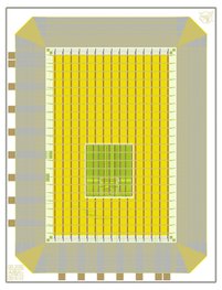
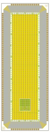
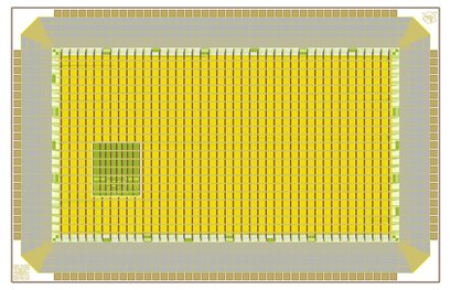
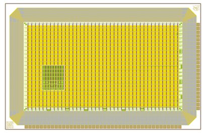
0.5×0.5 (Quarter)
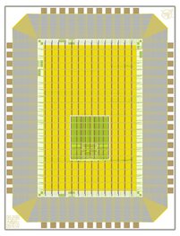
0.5×0.5 (Quarter)
Die Size
1.94mm × 2.53mm (4.90mm²)
Usable Silicon
1.88mm × 2.48mm (4.67mm²)
Core Area
1.05mm × 1.65mm (1.73mm²)
IO Overhead
65%
Total IOs
48 (bidir: 38, in: 6, analog: 4)
Power Pads
8 (4 DVDD + 4 DVSS)
Total Pads
56 (48 IO + 8 power)

0.5×0.5 2-side EXACT (Quarter, no north/east; pads pinned to slot_1x1 coords)

0.5×0.5 2-side EXACT (Quarter, no north/east; pads pinned to slot_1x1 coords)
Die Size
1.97mm × 2.56mm (5.03mm²)
Usable Silicon
1.91mm × 2.51mm (4.80mm²)
Core Area
1.08mm × 1.68mm (1.81mm²)
IO Overhead
64%
Total IOs
14 (bidir: 4, in: 8, analog: 2)
Power Pads
2 (1 DVDD + 1 DVSS)
Total Pads
16 (14 IO + 2 power)

0.5×1 3-side EXACT (Half Width, no east; pads pinned to slot_1x1 coords)

0.5×1 3-side EXACT (Half Width, no east; pads pinned to slot_1x1 coords)
Die Size
1.97mm × 5.12mm (10.07mm²)
Usable Silicon
1.91mm × 5.07mm (9.70mm²)
Core Area
1.08mm × 4.24mm (4.59mm²)
IO Overhead
54%
Total IOs
26 (bidir: 10, in: 14, analog: 2)
Power Pads
8 (4 DVDD + 4 DVSS)
Total Pads
34 (26 IO + 8 power)

1×0.5 3-side EXACT (Half Height, no north; pads pinned to slot_1x1 coords)

1×0.5 3-side EXACT (Half Height, no north; pads pinned to slot_1x1 coords)
Die Size
3.93mm × 2.56mm (10.07mm²)
Usable Silicon
3.88mm × 2.51mm (9.73mm²)
Core Area
3.05mm × 1.68mm (5.11mm²)
IO Overhead
49%
Total IOs
30 (bidir: 20, in: 8, analog: 2)
Power Pads
5 (2 DVDD + 3 DVSS)
Total Pads
35 (30 IO + 5 power)

Detailed Specifications

Slot Die Size Usable Silicon Core Area IO Overhead Bidir Inputs Analog Total IOs DVDD DVSS Power Pads Total Pads
1×1 (Full) 3.93 × 5.12mm
(20.14mm²)
3.88 × 5.07mm
(19.67mm²)
3.05 × 4.24mm
(12.92mm²)
36% 40 14 2 56 8 10 18 74
0.5×1 (Half Width) 1.94 × 5.12mm
(9.92mm²)
1.88 × 5.07mm
(9.55mm²)
1.05 × 4.24mm
(4.46mm²)
55% 44 6 6 56 8 8 16 72
1×0.5 (Half Height) 3.93 × 2.53mm
(9.95mm²)
3.88 × 2.48mm
(9.62mm²)
3.05 × 1.65mm
(5.02mm²)
50% 46 6 4 56 8 8 16 72
0.5×0.5 (Quarter) 1.94 × 2.53mm
(4.90mm²)
1.88 × 2.48mm
(4.67mm²)
1.05 × 1.65mm
(1.73mm²)
65% 38 6 4 48 4 4 8 56
0.5×0.5 2-side EXACT (Quarter, no north/east; pads pinned to slot_1x1 coords) 1.97 × 2.56mm
(5.03mm²)
1.91 × 2.51mm
(4.80mm²)
1.08 × 1.68mm
(1.81mm²)
64% 4 8 2 14 1 1 2 16
0.5×1 3-side EXACT (Half Width, no east; pads pinned to slot_1x1 coords) 1.97 × 5.12mm
(10.07mm²)
1.91 × 5.07mm
(9.70mm²)
1.08 × 4.24mm
(4.59mm²)
54% 10 14 2 26 4 4 8 34
1×0.5 3-side EXACT (Half Height, no north; pads pinned to slot_1x1 coords) 3.93 × 2.56mm
(10.07mm²)
3.88 × 2.51mm
(9.73mm²)
3.05 × 1.68mm
(5.11mm²)
49% 20 8 2 30 2 3 5 35
Download JSON

Understanding Slot Dimensions

Each slot has three important size measurements:

┌─────────────────────────────────────────┐
│             SEAL RING (26µm)            │
│  ┌───────────────────────────────────┐  │
│  │           IO RING                 │  │
│  │  ┌─────────────────────────────┐  │  │
│  │  │                             │  │  │
│  │  │        CORE AREA            │  │  │
│  │  │    (Your Design Area)       │  │  │
│  │  │                             │  │  │
│  │  └─────────────────────────────┘  │  │
│  │                                   │  │
│  └───────────────────────────────────┘  │
│                                         │
└─────────────────────────────────────────┘
 ◄─────────── DIE SIZE ──────────────────►
   ◄────── USABLE SILICON ────────────►
      ◄────── CORE SIZE ───────────►
                
Die Size
The actual physical silicon dimensions. This is the total area of the chip including all peripheral structures.
Usable Silicon
The die size minus the seal ring (26µm on each edge). The seal ring protects the chip from damage during dicing and provides a moisture barrier. This is the area available inside the seal ring.
Core Area
The usable design area inside the IO ring. This is where your digital logic, analog circuits, and other design elements are placed. The IO ring contains the pad cells that connect your design to the outside world.
3-Side Slot Configurations

Available Slots

Half-sized variants of the 1×1 slot. One edge is a bare cut edge with no IO pads, so the padring covers only three sides.

0.5×1 3-side (Half Width, no east)

0.5×1 3-side (Half Width, no east)
Die Size
1.97mm × 5.12mm (10.07mm²)
Usable Silicon
1.91mm × 5.07mm (9.70mm²)
Core Area
1.08mm × 4.24mm (4.59mm²)
IO Overhead
54%
Total IOs
30 (bidir: 14, in: 14, analog: 2)
Power Pads
10 (4 DVDD + 6 DVSS)
Total Pads
40 (30 IO + 10 power)

1×0.5 3-side (Half Height, no south)

1×0.5 3-side (Half Height, no south)
Die Size
3.93mm × 2.56mm (10.07mm²)
Usable Silicon
3.88mm × 2.51mm (9.73mm²)
Core Area
3.05mm × 1.68mm (5.11mm²)
IO Overhead
49%
Total IOs
30 (bidir: 20, in: 8, analog: 2)
Power Pads
9 (4 DVDD + 5 DVSS)
Total Pads
39 (30 IO + 9 power)

Detailed Specifications

Slot Die Size Usable Silicon Core Area IO Overhead Bidir Inputs Analog Total IOs DVDD DVSS Power Pads Total Pads
0.5×1 3-side (Half Width, no east) 1.97 × 5.12mm
(10.07mm²)
1.91 × 5.07mm
(9.70mm²)
1.08 × 4.24mm
(4.59mm²)
54% 14 14 2 30 4 6 10 40
1×0.5 3-side (Half Height, no south) 3.93 × 2.56mm
(10.07mm²)
3.88 × 2.51mm
(9.73mm²)
3.05 × 1.68mm
(5.11mm²)
49% 20 8 2 30 4 5 9 39

Advanced Slot Configurations

IO Configuration Options

Each slot can be configured with different IO pad densities and edge arrangements to suit your design needs.

Pad Density Modes

Choose how many IO pads you need:

Default (def)
Standard configuration with mixed pad types: bidirectional, input-only, and analog pads. Best for typical designs that need different pad characteristics.
Maximum (max)
Maximum number of pads possible for the slot size. All signal pads are bidirectional for maximum flexibility.
1x1 Spacing (spc)
Same pad spacing as the full 1x1 slot. Useful for maintaining consistent pad pitch across different slot sizes.
1x1 Count (num)
Same total pad count as the reference 1x1 slot. Ensures IO count compatibility when migrating designs.

Edge Configurations

Choose which edges have IO pads based on your slot position on the wafer:

All Edges (all)
IO pads on all four sides. Standard configuration for standalone designs.
Top Only (top)
IO pads only on the north edge. Ideal for slots positioned at the bottom of a multi-slot arrangement.
Left Only (lft)
IO pads only on the west edge. Ideal for slots positioned on the right side.
Horizontal (hor)
IO pads on north and south edges only. For slots that will connect to neighbors on left and right.
Vertical (ver)
IO pads on east and west edges only. For slots that will connect to neighbors above and below.
NW Corner (nwc)
IO pads on north and west edges. For slots positioned in the southeast corner of an arrangement.
SE Corner (sec)
IO pads on south and east edges. For slots positioned in the northwest corner of an arrangement.

Configuration Naming

Configurations are named using the pattern: {{slot}}_{{density}}_{{edges}}

Example: 0p5x0p5_max_all = 0.5×0.5 slot, maximum pads, all edges

Configuration Variants

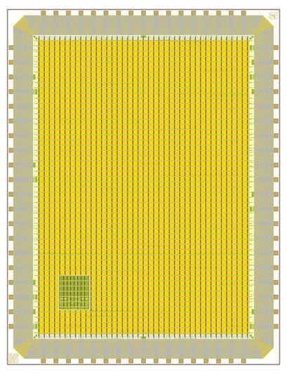
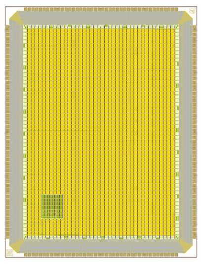
Each slot size has multiple configuration variants. Click on a slot to expand its variants. Click on images to view full size.

1×1 (Full) - 8 configurations
Diagram Image Config Name Density Edges Core Area Bidir DVDD DVSS Power Pads Total Pads
1x1_def_all 1x1_def_all Default All Edges 3.05 × 4.24mm 40 8 10 18 74
1x1_max_all 1x1_max_all Maximum All Edges 3.05 × 4.24mm 168 15 15 30 200
1x1_max_top 1x1_max_top Maximum Top Only 3.05 × 4.24mm 34 3 3 6 42
1x1_max_lft 1x1_max_lft Maximum Left Only 3.05 × 4.24mm 48 4 4 8 58
1x1_max_hor 1x1_max_hor Maximum Horizontal 3.05 × 4.24mm 70 6 6 12 84
1x1_max_ver 1x1_max_ver Maximum Vertical 3.05 × 4.24mm 96 9 9 18 116
1x1_max_nwc 1x1_max_nwc Maximum NW Corner 3.05 × 4.24mm 84 7 7 14 100
1x1_max_sec 1x1_max_sec Maximum SE Corner 3.05 × 4.24mm 84 7 7 14 100
0.5×1 (Half Width) - 22 configurations
Diagram Image Config Name Density Edges Core Area Bidir DVDD DVSS Power Pads Total Pads
0p5x1_def_all 0p5x1_def_all Default All Edges 1.05 × 4.24mm 44 8 8 16 72
0p5x1_max_all 0p5x1_max_all Maximum All Edges 1.05 × 4.24mm 122 11 11 22 146
0p5x1_max_top 0p5x1_max_top Maximum Top Only 1.05 × 4.24mm 11 1 1 2 15
0p5x1_max_lft 0p5x1_max_lft Maximum Left Only 1.05 × 4.24mm 48 4 4 8 58
0p5x1_max_hor 0p5x1_max_hor Maximum Horizontal 1.05 × 4.24mm 24 2 2 4 30
0p5x1_max_ver 0p5x1_max_ver Maximum Vertical 1.05 × 4.24mm 96 9 9 18 116
0p5x1_max_nwc 0p5x1_max_nwc Maximum NW Corner 1.05 × 4.24mm 61 5 5 10 73
0p5x1_max_sec 0p5x1_max_sec Maximum SE Corner 1.05 × 4.24mm 61 5 5 10 73
0p5x1_spc_all 0p5x1_spc_all 1x1 Spacing All Edges 1.05 × 4.24mm 122 11 11 22 146
0p5x1_spc_top 0p5x1_spc_top 1x1 Spacing Top Only 1.05 × 4.24mm 11 1 1 2 15
0p5x1_spc_lft 0p5x1_spc_lft 1x1 Spacing Left Only 1.05 × 4.24mm 48 4 4 8 58
0p5x1_spc_hor 0p5x1_spc_hor 1x1 Spacing Horizontal 1.05 × 4.24mm 24 2 2 4 30
0p5x1_spc_ver 0p5x1_spc_ver 1x1 Spacing Vertical 1.05 × 4.24mm 96 9 9 18 116
0p5x1_spc_nwc 0p5x1_spc_nwc 1x1 Spacing NW Corner 1.05 × 4.24mm 61 5 5 10 73
0p5x1_spc_sec 0p5x1_spc_sec 1x1 Spacing SE Corner 1.05 × 4.24mm 61 5 5 10 73
0p5x1_num_all 0p5x1_num_all 1x1 Count All Edges 1.05 × 4.24mm 62 5 5 10 74
0p5x1_num_top 0p5x1_num_top 1x1 Count Top Only 1.05 × 4.24mm 11 1 1 2 15
0p5x1_num_lft 0p5x1_num_lft 1x1 Count Left Only 1.05 × 4.24mm 48 4 4 8 58
0p5x1_num_hor 0p5x1_num_hor 1x1 Count Horizontal 1.05 × 4.24mm 24 2 2 4 30
0p5x1_num_ver 0p5x1_num_ver 1x1 Count Vertical 1.05 × 4.24mm 62 5 5 10 74
0p5x1_num_nwc 0p5x1_num_nwc 1x1 Count NW Corner 1.05 × 4.24mm 61 5 5 10 73
0p5x1_num_sec 0p5x1_num_sec 1x1 Count SE Corner 1.05 × 4.24mm 61 5 5 10 73
1×0.5 (Half Height) - 22 configurations
Diagram Image Config Name Density Edges Core Area Bidir DVDD DVSS Power Pads Total Pads
1x0p5_def_all 1x0p5_def_all Default All Edges 3.05 × 1.65mm 46 8 8 16 72
1x0p5_max_all 1x0p5_max_all Maximum All Edges 3.05 × 1.65mm 108 10 10 20 130
1x0p5_max_top 1x0p5_max_top Maximum Top Only 3.05 × 1.65mm 34 3 3 6 42
1x0p5_max_lft 1x0p5_max_lft Maximum Left Only 3.05 × 1.65mm 17 2 2 4 23
1x0p5_max_hor 1x0p5_max_hor Maximum Horizontal 3.05 × 1.65mm 70 6 6 12 84
1x0p5_max_ver 1x0p5_max_ver Maximum Vertical 3.05 × 1.65mm 38 3 3 6 46
1x0p5_max_nwc 1x0p5_max_nwc Maximum NW Corner 3.05 × 1.65mm 53 5 5 10 65
1x0p5_max_sec 1x0p5_max_sec Maximum SE Corner 3.05 × 1.65mm 53 5 5 10 65
1x0p5_spc_all 1x0p5_spc_all 1x1 Spacing All Edges 3.05 × 1.65mm 108 10 10 20 130
1x0p5_spc_top 1x0p5_spc_top 1x1 Spacing Top Only 3.05 × 1.65mm 34 3 3 6 42
1x0p5_spc_lft 1x0p5_spc_lft 1x1 Spacing Left Only 3.05 × 1.65mm 17 2 2 4 23
1x0p5_spc_hor 1x0p5_spc_hor 1x1 Spacing Horizontal 3.05 × 1.65mm 70 6 6 12 84
1x0p5_spc_ver 1x0p5_spc_ver 1x1 Spacing Vertical 3.05 × 1.65mm 38 3 3 6 46
1x0p5_spc_nwc 1x0p5_spc_nwc 1x1 Spacing NW Corner 3.05 × 1.65mm 53 5 5 10 65
1x0p5_spc_sec 1x0p5_spc_sec 1x1 Spacing SE Corner 3.05 × 1.65mm 53 5 5 10 65
1x0p5_num_all 1x0p5_num_all 1x1 Count All Edges 3.05 × 1.65mm 62 5 5 10 74
1x0p5_num_top 1x0p5_num_top 1x1 Count Top Only 3.05 × 1.65mm 34 3 3 6 42
1x0p5_num_lft 1x0p5_num_lft 1x1 Count Left Only 3.05 × 1.65mm 17 2 2 4 23
1x0p5_num_hor 1x0p5_num_hor 1x1 Count Horizontal 3.05 × 1.65mm 62 5 5 10 74
1x0p5_num_ver 1x0p5_num_ver 1x1 Count Vertical 3.05 × 1.65mm 38 3 3 6 46
1x0p5_num_nwc 1x0p5_num_nwc 1x1 Count NW Corner 3.05 × 1.65mm 53 5 5 10 65
1x0p5_num_sec 1x0p5_num_sec 1x1 Count SE Corner 3.05 × 1.65mm 53 5 5 10 65
0.5×0.5 (Quarter) - 22 configurations
Diagram Image Config Name Density Edges Core Area Bidir DVDD DVSS Power Pads Total Pads
0p5x0p5_def_all 0p5x0p5_def_all Default All Edges 1.05 × 1.65mm 38 4 4 8 56
0p5x0p5_max_all 0p5x0p5_max_all Maximum All Edges 1.05 × 1.65mm 62 6 6 12 76
0p5x0p5_max_top 0p5x0p5_max_top Maximum Top Only 1.05 × 1.65mm 11 1 1 2 15
0p5x0p5_max_lft 0p5x0p5_max_lft Maximum Left Only 1.05 × 1.65mm 17 2 2 4 23
0p5x0p5_max_hor 0p5x0p5_max_hor Maximum Horizontal 1.05 × 1.65mm 24 2 2 4 30
0p5x0p5_max_ver 0p5x0p5_max_ver Maximum Vertical 1.05 × 1.65mm 38 3 3 6 46
0p5x0p5_max_nwc 0p5x0p5_max_nwc Maximum NW Corner 1.05 × 1.65mm 30 3 3 6 38
- 0p5x0p5_max_sec Maximum SE Corner 1.05 × 1.65mm 30 3 3 6 38
0p5x0p5_spc_all 0p5x0p5_spc_all 1x1 Spacing All Edges 1.05 × 1.65mm 62 6 6 12 76
0p5x0p5_spc_top 0p5x0p5_spc_top 1x1 Spacing Top Only 1.05 × 1.65mm 11 1 1 2 15
0p5x0p5_spc_lft 0p5x0p5_spc_lft 1x1 Spacing Left Only 1.05 × 1.65mm 17 2 2 4 23
0p5x0p5_spc_hor 0p5x0p5_spc_hor 1x1 Spacing Horizontal 1.05 × 1.65mm 24 2 2 4 30
0p5x0p5_spc_ver 0p5x0p5_spc_ver 1x1 Spacing Vertical 1.05 × 1.65mm 38 3 3 6 46
0p5x0p5_spc_nwc 0p5x0p5_spc_nwc 1x1 Spacing NW Corner 1.05 × 1.65mm 30 3 3 6 38
0p5x0p5_spc_sec 0p5x0p5_spc_sec 1x1 Spacing SE Corner 1.05 × 1.65mm 30 3 3 6 38
0p5x0p5_num_all 0p5x0p5_num_all 1x1 Count All Edges 1.05 × 1.65mm 61 5 5 10 73
0p5x0p5_num_top 0p5x0p5_num_top 1x1 Count Top Only 1.05 × 1.65mm 11 1 1 2 15
0p5x0p5_num_lft 0p5x0p5_num_lft 1x1 Count Left Only 1.05 × 1.65mm 17 2 2 4 23
0p5x0p5_num_hor 0p5x0p5_num_hor 1x1 Count Horizontal 1.05 × 1.65mm 24 2 2 4 30
0p5x0p5_num_ver 0p5x0p5_num_ver 1x1 Count Vertical 1.05 × 1.65mm 38 3 3 6 46
0p5x0p5_num_nwc 0p5x0p5_num_nwc 1x1 Count NW Corner 1.05 × 1.65mm 30 3 3 6 38
0p5x0p5_num_sec 0p5x0p5_num_sec 1x1 Count SE Corner 1.05 × 1.65mm 30 3 3 6 38
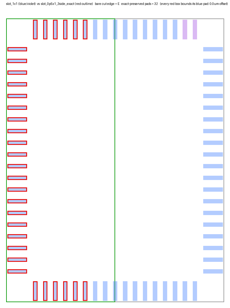
Exact-Pad 3-Side Verification

slot_1x1 vs Exact 3-Side Pad Overlay

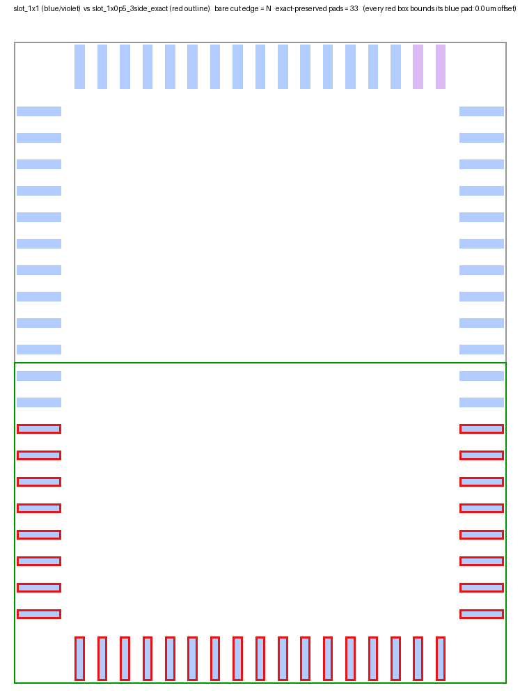
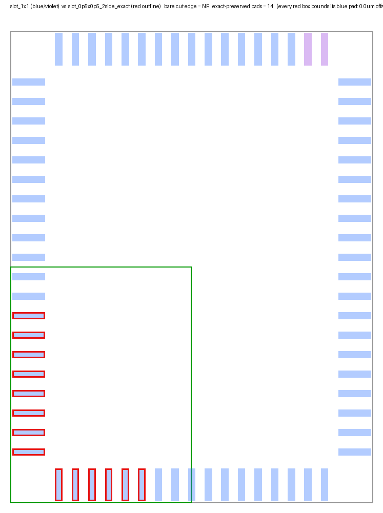
The *_3side_exact configs pin every retained signal/power pad (via a custom PAD_CFG) to the exact (x, y) it occupies in a real slot_1x1 build. Below, blue = slot_1x1 pads, red outline = the exact 3-side pads. Every red box bounds its blue pad with a verified 0.0 µm offset; blue-only pads sit across the bare cut edge and are intentionally dropped.
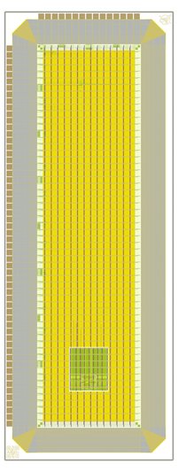
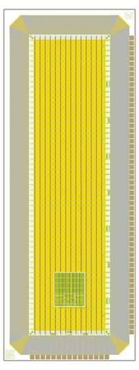
0.5×1 3-side EXACT (half width, east edge is the bare cut)

0p5x1_3side_exact overlay

1×0.5 3-side EXACT (half height, north edge is the bare cut)

1x0p5_3side_exact overlay

0.5×0.5 2-side EXACT (quarter, north + east edges are the bare cuts)

0p5x0p5_2side_exact overlay